高亮液晶屏
TFT触摸屏
HDMI TFT显示器
工业级TFT屏
OLED屏
条型TFT屏
圆形TFT屏
方形TFT屏
全视角TFT屏
电阻触摸TFT屏
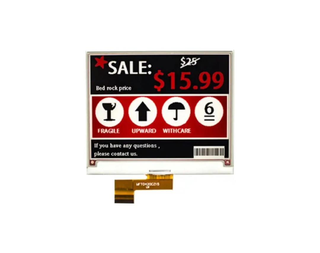
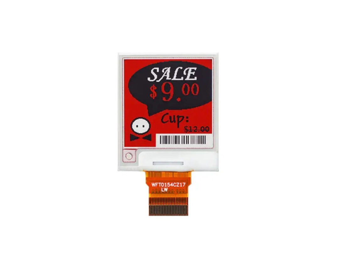
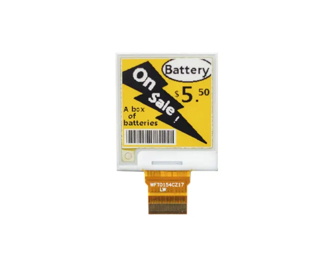
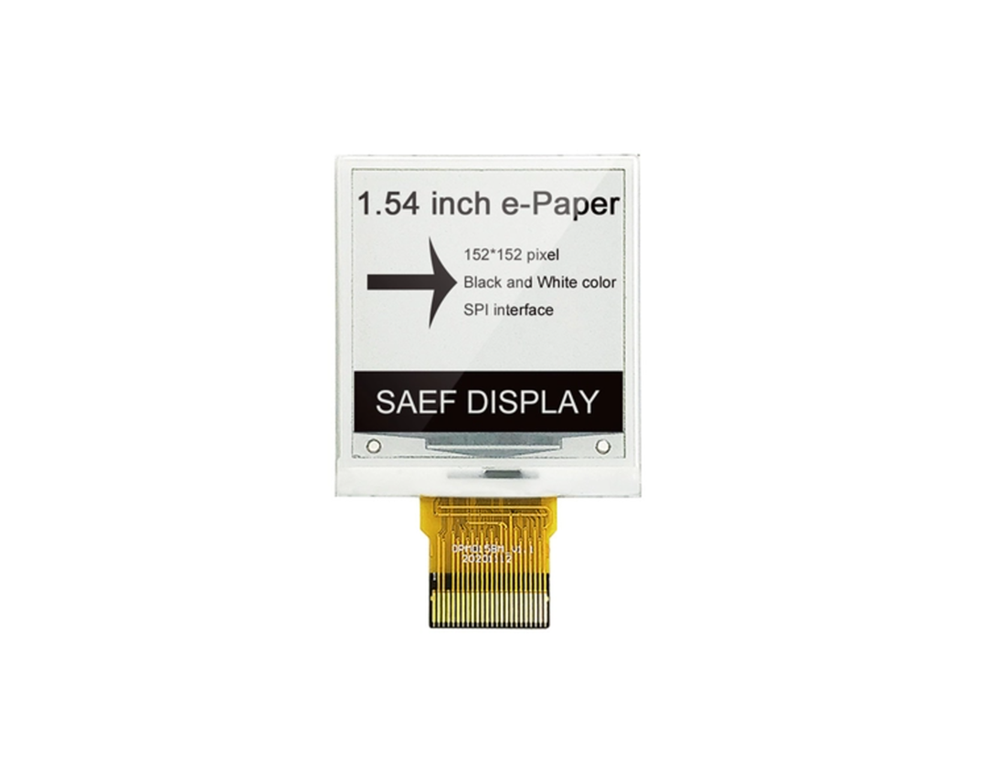
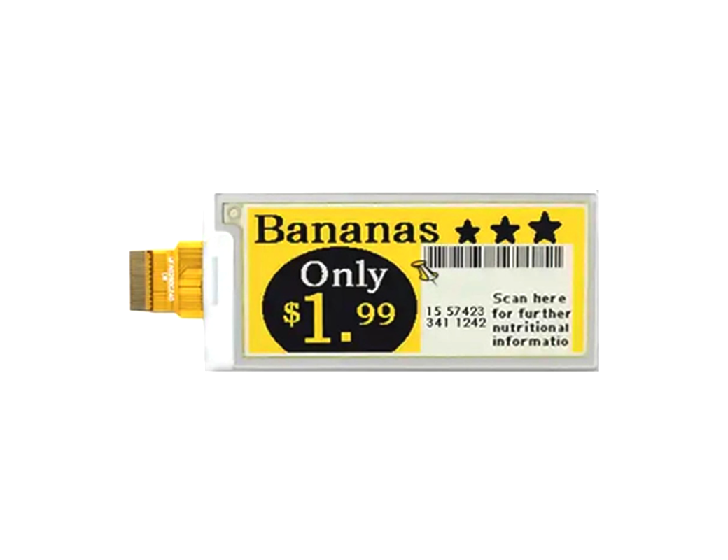
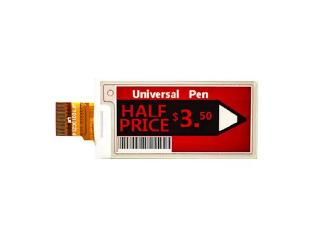
电子墨水屏
树莓派触摸屏
OLED模块
高亮液晶屏
TFT触摸屏
HDMI TFT显示器
工业级TFT屏
OLED屏
条型TFT屏
圆形TFT屏
方形TFT屏
全视角TFT屏
电阻触摸TFT屏
电子墨水屏
树莓派触摸屏
OLED模块

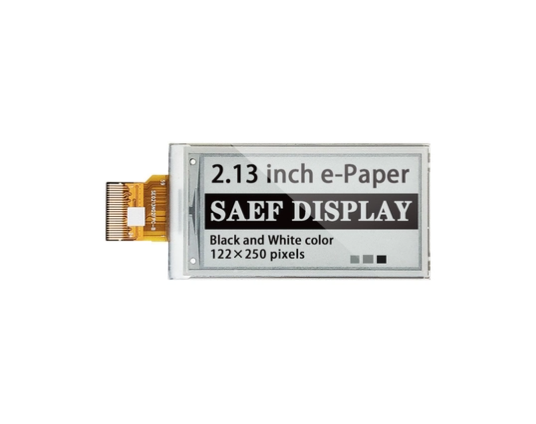
产品概述
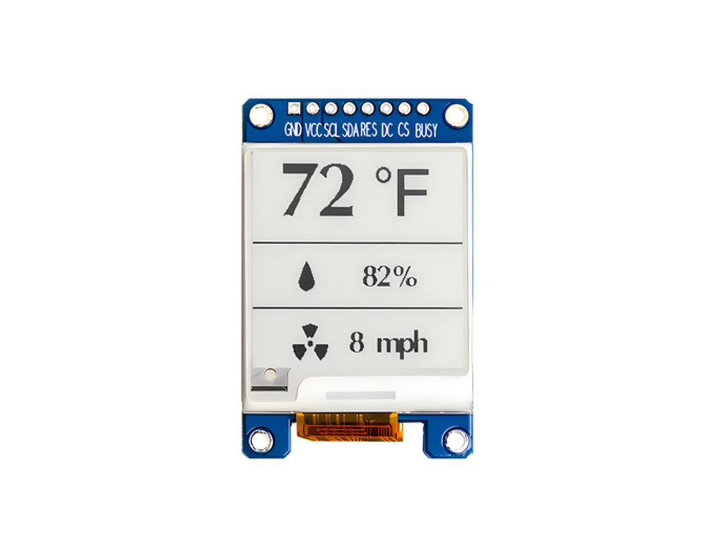
使用 SFEPD213BWY-7018A01 升级您的显示器,这是一款多功能的 2.13 英寸电子纸显示器,具有三种颜色(白色、黑色和红色)。这款高分辨率 (131dpi) 屏幕具有以下特点:
· 节能:超低功耗。显示器仅在图像变化时才耗电,无需任何电源来维持。
· 卓越的可读性:超宽视角(接近 180°)确保从任何方向都能清晰显示。
· 时尚设计:超薄超轻,非常适合集成到各种设备中。
· 轻松连接:SPI 接口可实现无缝兼容。
· 环保意识:符合 RoHS 标准。
主要应用:
· 电子货架标签:创建动态、醒目的价格和产品信息显示。
· 电子阅读器:享受纸质阅读体验。
· 电子笔记本:以自然的感觉记录笔记和草图。
· 可穿戴设备:将信息显示集成到紧凑型设备中。
· 还有更多!
产品规格
| Product: | EPD 2.13″ inch |
| Resolution: | 122×250 Dots Resolution |
| Display Mode: | Active Matrix Electrophoretic Display(AM EPD) |
| Optics: | All Viewing Angles |
| Outline Dim.: | 29.2(H)x59.2(V)x1.0(D) Mm |
| Active Area: | 23.705(H)x48.55(V) Mm |
| Operating Temp: | 0°C To +50°C |
| Storage Temp: | -25°C To +60°C |
| Pin Number: | 24 Pins |
| Interface: | SPI |
外形结构图

接口引脚定义
| No. | Signal | Type | Connected to | Function |
| 1 | NC | – | – | Not connected |
| 2 | GDR | O | Power MOSFET Driver control | This pin is the N-Channel MOSFET Gate Drive Control. |
| 3 | RESE | I | Booster Control Input | This pin is the Current Sense Input for the Control Loop. |
| 4 | NC | – | – | Not connected |
| 5 | VSHR | C | Capacitor | This pin is the Positive Gate driving voltage and the Power Supply pin for VSH2. A stabilizing capacitor should be connected between VSH2 and GND. |
| 6 | TSCL(NC) | – | – | – |
| 7 | TSDA(NC) | – | – | – |
| 8 | BS | I | VSS | This pin is setting panel interface. |
| 9 | BUSY | O | Device Busy Signal | This pin is Busy state output pin. When Busy is High, the operation of the chip should not be interrupted, and Command should not be sent. |
| 10 | RES_N | I | System Reset | This pin is reset signal input.Active Low. |
| 11 | D/C | I | VDDIO or VSS | This pin is Data/Command control |
| 12 | CSB | I | VDDIO or VSS | This pin is the chip select. |
| 13 | SCL | I | Data Bus | Serial communication clock input. |
| 14 | SDA | I | Data Bus | Serial communication data input/output. |
| 15 | VDDIO | P | Power Supply | Power for interface logic pins& I/O. It should be connected with VCI. |
| 16 | VCI | P | Power Supply | Power Supply for the chip. |
| 17 | GND | P | Ground | Ground |
| 18 | VDDD | C | Capacitor | Internal regulator output. A capacitor should be connected between VDD and GND. |
| 19 | VPP(NC) | – | – | – |
| 20 | VSH | C | Capacitor | This pin is the Positive Source driving voltage. A stabilizing capacitor should be connected between VSH and GND. |
| 21 | VGH | C | Capacitor | A stabilizing capacitor should be connected between VGH and GND. |
| 22 | VSL | C | Capacitor | This pin is the Negative Source driving voltage and the Power Supply pin for VCOM. A stabilizing capacitor should be connected between VSL and GND. |
| 23 | VGL | C | Capacitor | A stabilizing capacitor should be connected between VGL and GND. |
| 24 | VCOM | C | Capacitor | This pin is the VCOM driving voltage. A stabilizing capacitor should be connected between VCOM and GND. |
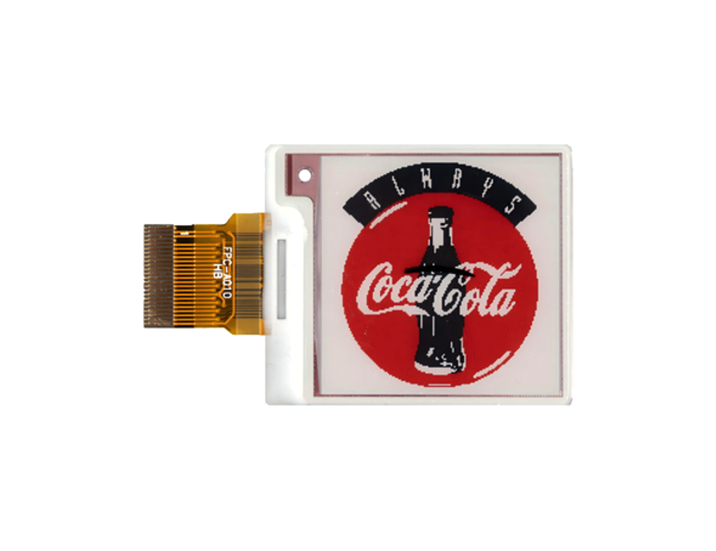
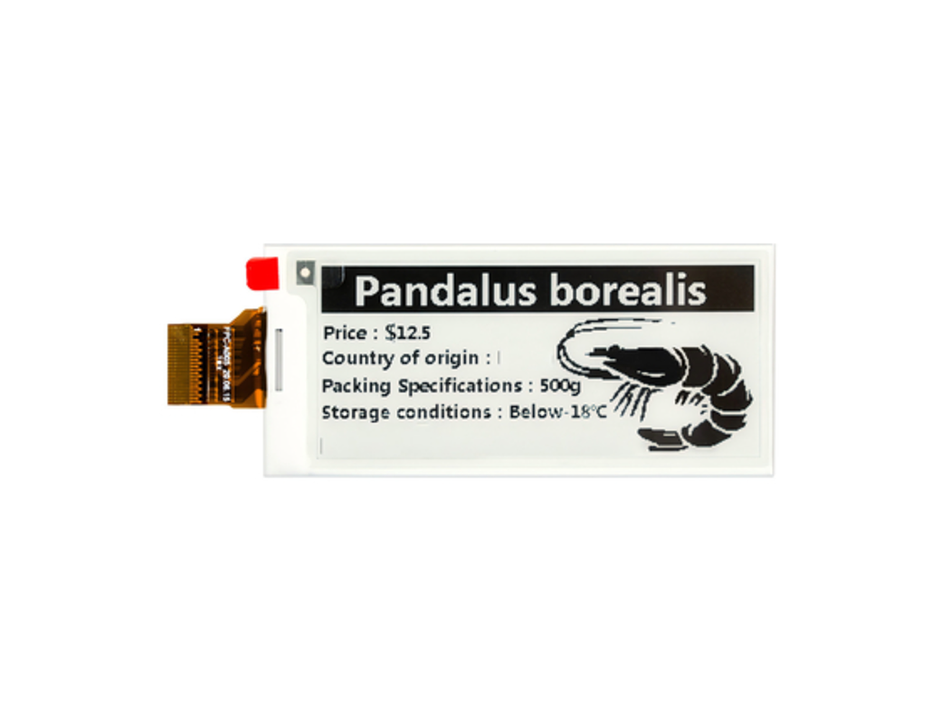
产品图像


手机/微信:135 0298 3321 柯先生
手机/微信:138 2960 7086 郑小姐
手机/微信:136 8686 7235 陈小姐
地址: 深圳市宝安区洲石路阳光工业区D栋


在线留言

 135 0298 3321
 首页 》
首页 》