高亮液晶屏
TFT触摸屏
HDMI TFT显示器
工业级TFT屏
OLED屏
条型TFT屏
圆形TFT屏
方形TFT屏
全视角TFT屏
电阻触摸TFT屏
电子墨水屏
树莓派触摸屏
OLED模块
高亮液晶屏
TFT触摸屏
HDMI TFT显示器
工业级TFT屏
OLED屏
条型TFT屏
圆形TFT屏
方形TFT屏
全视角TFT屏
电阻触摸TFT屏
电子墨水屏
树莓派触摸屏
OLED模块

产品概述
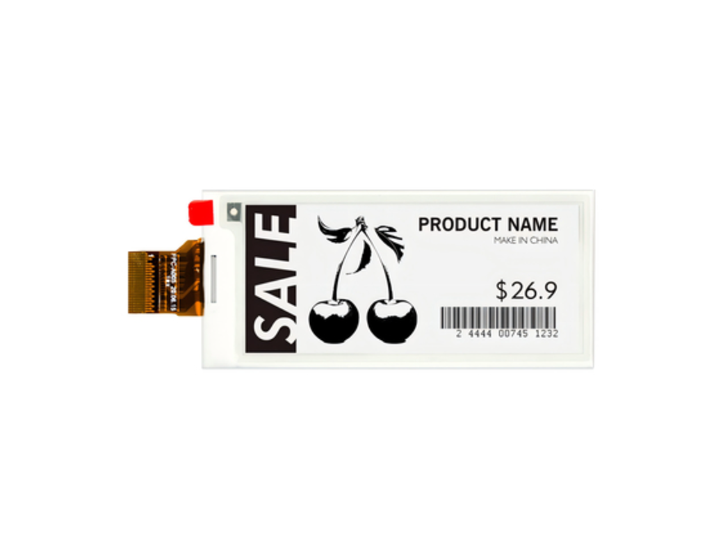
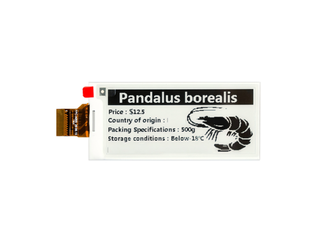
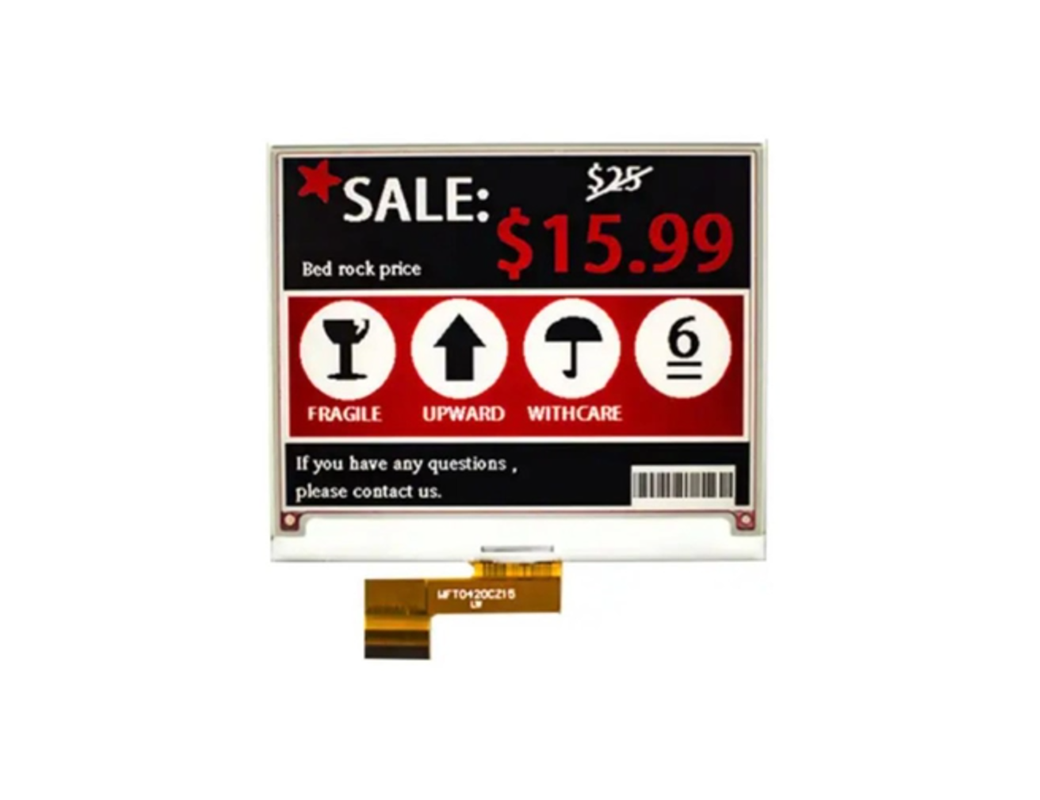
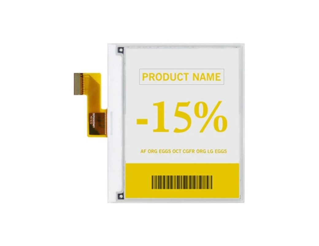
说明:这款 a-Si TFT 有源矩阵电子墨水屏SFEPD420BWR-7021A01提供 400×300 分辨率、黑色、白色和红色显示,并且功耗非常低。非常适合需要持久、易读显示屏的应用。
规格:
· 类型:a-Si TFT 有源矩阵 EPD
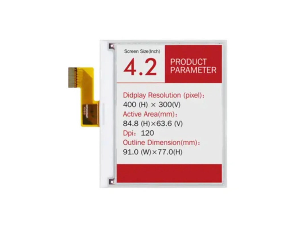
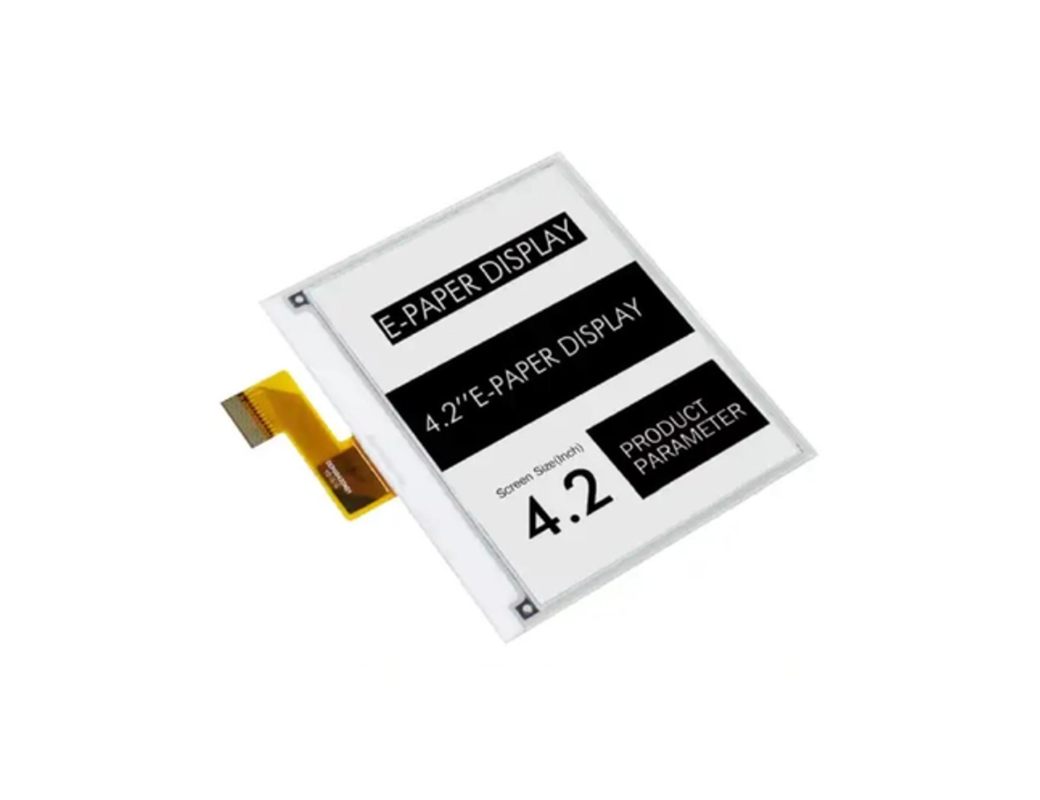
· 尺寸:4.2 英寸
· 分辨率:400×300
· 颜色:黑色、白色、红色
· 视角:接近 180°
· 接口:SPI
· 符合 RoHS 标准
主要规格
| Product: | 4.2-Inch Color E-Ink EPaper Display |
| Resolution: | 400 X300 Dots Resolution |
| Display Mode: | Active Matrix Electrophoretic Display (AM EPD) |
| Optics: | All Viewing Angles |
| Outline Dim.: | 91 (H) X 77(V)x 0.9(T) Mm |
| Active Area: | 84.8 (H) X 63.6(V) Mm |
| Pixel Pitch: | 0.212x 0.212 (120dpi) |
| Operating Temp: | 0°C To +40°C |
| Storage Temp: | -25°C To +60°C |
| Color: | Black/White/Red |
| Surface Treatment: | Anti-Glare, 3H |
| Pin Number: | 24 Pins |
| Interface: | SPI |
| Pixel Arrangement: | Vertical Stripe |
| Input Current: | 4.93 MA |
| Compliance: | Rohs & Reach Compliant |
外形结构图

接口引脚定义
| No. | Name | I/O | Description | Remark |
| 1 | NC | Do not connect with other NC pins | ||
| 2 | GDR | O | N-Channel MOSFET Gate Drive Control | |
| 3 | RESE | I | Current Sense Input for the Control Loop | |
| 4 | NC | Do not connect with other NC pins | ||
| 5 | VDHR | C | Positive Source driving voltage 1 | |
| 6 | TSCL | O | I2C Interface to digital temperature sensor Clock pin | |
| 7 | TSDA | I/O | I2C Interface to digital temperature sensor Data pin | |
| 8 | BS | I | Bus Interface selection pin | Note 5-4 |
| 9 | BUSYN | O | Busy state output pin | Note 5-3 |
| 10 | RSTN | I | Reset signal input. Active Low. | |
| 11 | D/C | I | Data /Command control pin | Note 5-2 |
| 12 | CSB | I | Chip select input pin | Note 5- 1 |
| 13 | SCL | I | Serial Clock pin (SPI) | |
| 14 | SDA | I | Serial Data pin (SPI) | |
| 15 | VDD | P | Power Supply for interface logic pins | |
| 16 | VDD | P | Power Supply for the chip | |
| 17 | VSS | P | Ground | |
| 18 | VDDD | C | Core logic power pin. VDDD can be regulated internally from VDD. A capacitor should be connected between VDDD and VSS under all circumstances. | |
| 19 | VPP | P | Power Supply for OTP Programming | |
| 20 | VSH | C | Positive Source driving voltage | |
| 21 | VGH | C | Positive Gate driving voltage | |
| 22 | VSL | C | Negative Source driving voltage | |
| 23 | VGL | C | Negative Gate driving voltage | |
| 24 | VCOM | C | VCOM driving voltage |
绝对最大额定值
| Parameter | Symbol | Rating | Unit |
| Logic supply voltage | Vdd | -0.5 to +4.0 | V |
| Logic Input voltage | VIN | -0.5 to Vdd +0.5 | V |
| Logic Output voltage | VOUT | -0.5 to Vdd +0.5 | V |
直流特性
以下规格适用于:VSS=0V、VDD=3.0V、TOPR =25ºC。
| Parameter | Symbol | Condition | Applicable pin | Min. | Typ. | Max. | Unit |
| Logic supply voltage | Vdd | – | VDD | 2.4 | 3.0 | 3.6 | V |
| High level input voltage | VIH | – | – | 0.8 Vdd | – | – | V |
| Low level input voltage | VIL | – | – | – | – | 0.2 Vdd | V |
| High level output voltage | VOH | IOH = – 100uA | – | 0.9 Vdd | – | – | V |
| Low level output voltage | VOL | IOL = 100uA | – | – | – | 0.1 Vdd | V |
| Typical power panel | PTYP | – | – | – | 45 | 240 | mW |
| Deep sleep mode | PSTPY | – | – | – | 3 | – | uW |
| Typical operating current | Iopr_VDD | Vdd =3.0V | – | – | 15 | 80 | mA |
| Sleep mode current | Islp_VDD | VDD=3.0V DC/DC OFF No clock, No output load Ram data retain. | VDD | – | 35 | 50 | uA |
| Deep sleep mode current | Idslp VDD | VDD=3.0V DC/DC OFF No clock No output load Ram data not retain | VDD | – | 1 | – | uA |
| Operation temperature | TOPR | – | – | 0 | – | 50 | °C |
| Operation relative humidity | RHop | – | – | – | – | 70 | %RH |
| Operation illuminance intensity | E | indoor only | – | – | – | 2000 | lux |
| Storage temperature | TSTG | – | – | -25 | – | 60 | °C |
| Storage relative humidity | RHst | – | – | 30 | – | 60 | %RH |
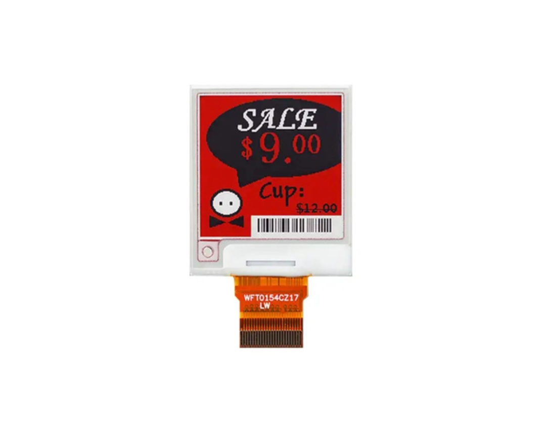
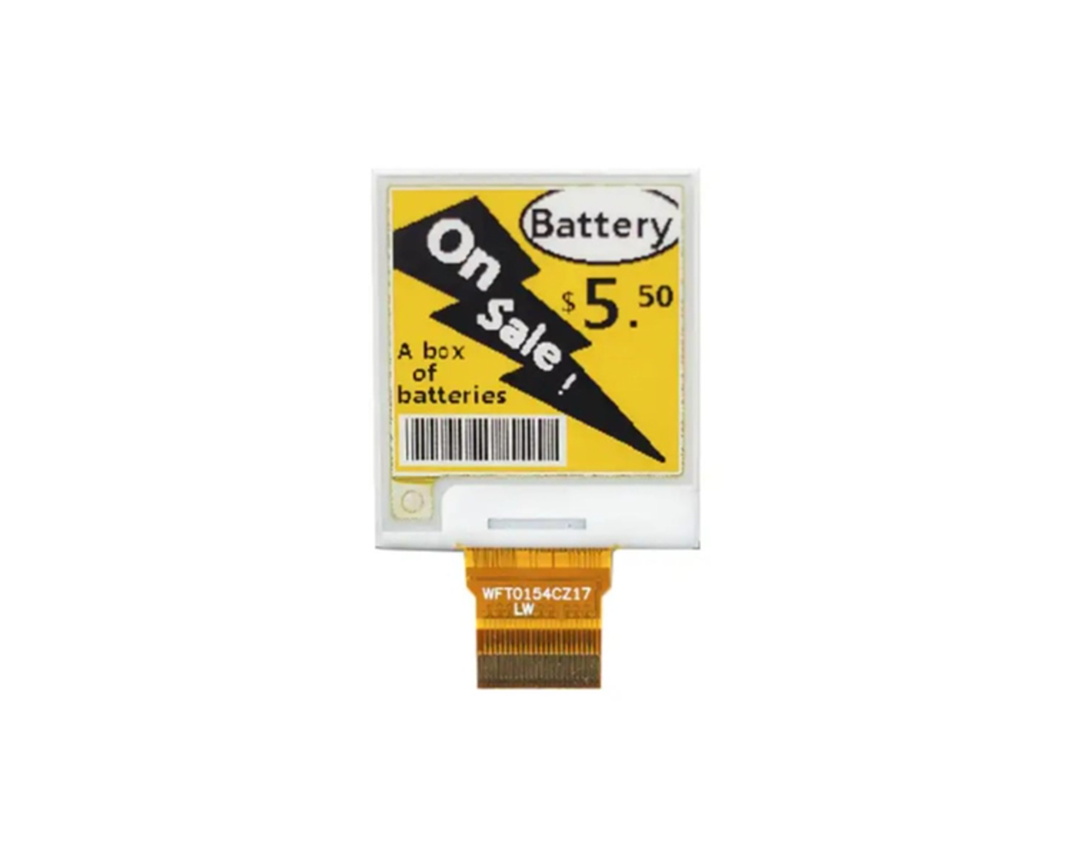
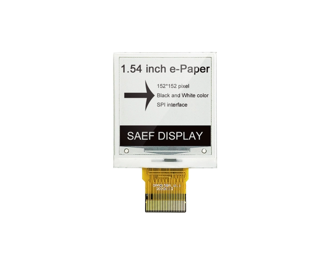
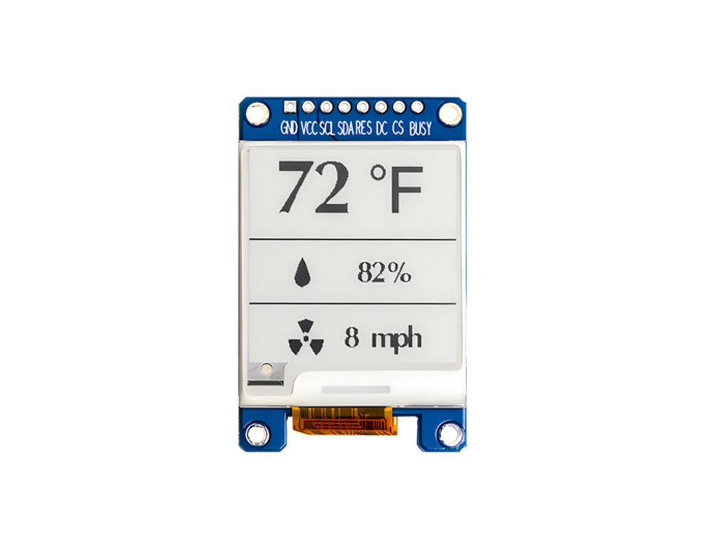
产品图片


手机/微信:135 0298 3321 柯先生
手机/微信:138 2960 7086 郑小姐
手机/微信:136 8686 7235 陈小姐
地址: 深圳市宝安区洲石路阳光工业区D栋


在线留言

 135 0298 3321
 首页 》
首页 》