高亮液晶屏
TFT触摸屏
HDMI TFT显示器
工业级TFT屏
OLED屏
条型TFT屏
圆形TFT屏
方形TFT屏
全视角TFT屏
电阻触摸TFT屏
电子墨水屏
树莓派触摸屏
OLED模块
高亮液晶屏
TFT触摸屏
HDMI TFT显示器
工业级TFT屏
OLED屏
条型TFT屏
圆形TFT屏
方形TFT屏
全视角TFT屏
电阻触摸TFT屏
电子墨水屏
树莓派触摸屏
OLED模块

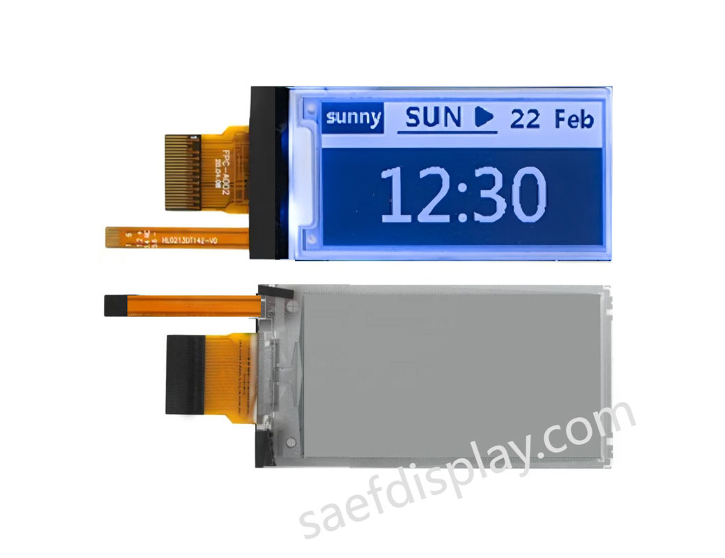
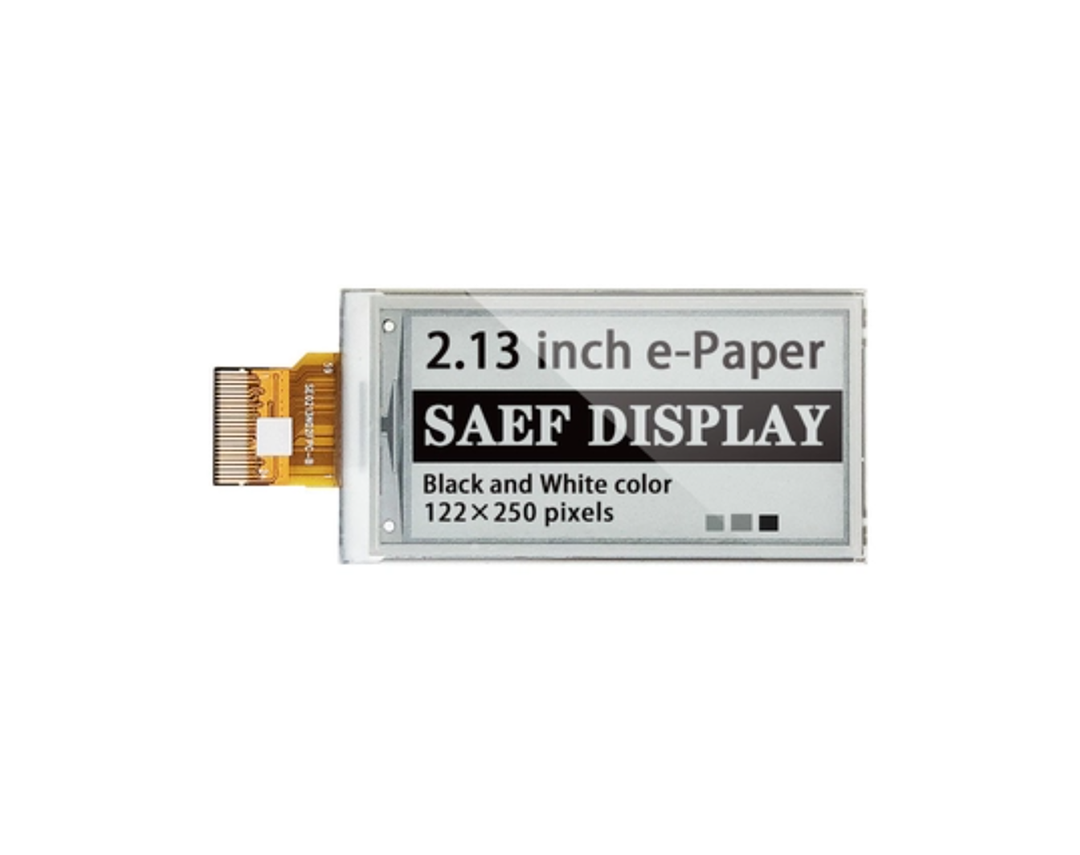
| Technology: | Electrophoretic E-ink (Bi-stable) | Screen Size: | 2.13 Inch (54.1 Mm Diagonal) |
| Special Features:: | Integrated Frontlight | Resolution: | 122 (H) × 250 (V) Pixels | 130 DPI |
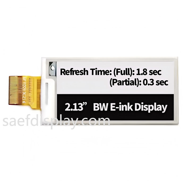
| Interface: | Configurable SPI (3-w/4-w Via BS1 Pin) | Refresh Time: | Full Update: 1.8 Sec; Partial Update: 0.3 Sec |
| Active Area: | 23.7 × 48.55 (mm) | Color: | Monochrome (Black/White) |
| Power Supply: | 10.5 MW (Typ.) | Viewing Angle: | 180° (Ultra-wide) |
| Optical: | Reflectivity: 35% (Typ.) | Operating Temp: | 0°C To +50°C |
| Storage Temp.: | -25°C To +60°C | Compliance: | REACH & RoHS Compliant & Halogen Free |
| Customization:: | CTP Optional Via I²C, OCA Lamination Support | Reliability: | Validated For 240 Hrs At 90% RH, ±8kV ESD, UV Exposure |
| Highlight: | 2.13 inch E Ink display module, ultra-low power e-paper display, industrial-grade SPI e-paper module | ||
恶劣环境的工业级墨水显示
SFE213RJBW-7307A是一款2.13英寸单色电泳显示(EPD),该显示为苛刻的工业应用,包括电子架子标签(ESL),便携式医疗设备和IoT Edge Systems。使用超低的深度睡眠电流(<1μA)和可配置的SPI接口(4线或3线),该模块可实现多年的电池寿命,同时最大程度地减少MCU资源开销。
工厂集成的精密工程
可靠性:根据IEC 60068-2验证热冲击标准(-25°C +70°C),湿度(90%RH)和振动。
供应链稳定性:在中国深圳经过ISO 9001/14001认证的设施中制造,可追溯的组件采购(Taiyo Yuden电感器,Onsemi Diodes)。
设计支持:包括参考电路(第19页),LUT波形和交流正时图(第13页),用于快速PCB集成。
技术差异与通用显示
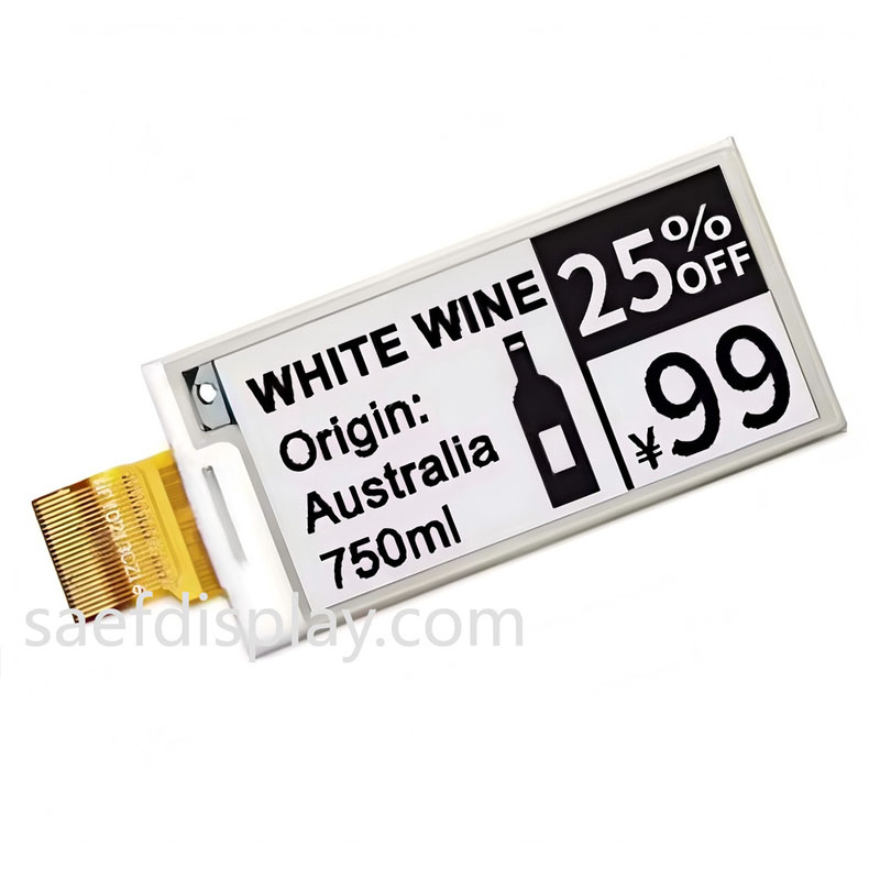
部分刷新(0.3s):对于动态ESL价格更新的完整刷新(1.8s)6倍。
芯片电源管理:VCOM,VGH,VGL的集成助推器/调节器 - 无需外部PMIC。
ESD硬化:IEC61000-4-2符合工厂处理鲁棒性的IEC61000-4-2(4KV触点/8KV空气)。
我们/德国工程团队的理想选择
自动化ESL系统:SPI Daisy Chains Charing Support for大规模部署。
医疗/物流工具:宽温度范围(-25°C至 +60°C的存储空间),以进行冷链合规性。
寿命的重点:50,000多个更新周期,具有双稳定的零功率图像保留。
订购与合规性
欧文:1,000个单位(可自定义量)。
交货时间:4–6周(欧盟/美国的空运)。
文档:完整覆盖范围/ROHS测试报告,符合IPC的包装(480pcs/box)。
▶在此页面中下载数据表。
▶请求CTP样本:具有20天提前时间的自定义触摸解决方案。
机械尺寸

机械规格
| Parameter | Specifications | Unit | Remark |
| Screen Size | 2.13 | Inch | |
| Display Resolution | 122(H)×250(V) | Pixel | Dpi:130 |
| Active Area | 23.7×48.55 | mm | |
| Pixel Pitch | 0. 1943×0.1942 | mm | |
| Pixel Configuration | Retangle | ||
| Outline Dimension | 29.2(H)×59.2 (V) ×0.9(D) | mm | |
| Weight | TBD | g |
绝对最大额定值
| Parameter | Symbol | Rating | Unit |
| Logic supply voltage | VCI | -0.3 to +6.0 | V |
| Logic Input voltage | VIN | -0.3 to VCI +0.3 | V |
| Logic Output voltage | VOUT | -0.3 to VCI +0.3 | V |
| Operating Temp range | TOPR | 0 to +50 | ºC |
| Storage Temp range | TSTG | -25 to+60 | ºC |
| Optimal Storage Temp | TSTGo | 23±2 | ºC |
| Opt ma Storage Hum ty | HSTGo | 55±10 | RH |
面板直流特征
| Parameter | Symbol | Condition | Min. | Typ. | Max. | Unit |
| Single ground | GND | - | - | 0 | - | V |
| IO Supply Voltage | VDDIO | - | 2.3 | 3.3 | 3.6 | V |
| Digital/Analog supply voltage | VDD | - | 2.3 | 3.3 | 3.6 | V |
| High level input voltage | Vih | - | 0.7VDDIO | - | VDDIO | V |
| Low level input voltage | Vil | - | 0 | - | 0.3VDDIO | V |
| High level output voltage | Voh | IOH = 400uA | VDDIO-0.4 | - | - | V |
| Low level output voltage | Vol | IOL = -400uA | 0 | - | 0.4 | V |
| OTP program power | VPP | - | 7.5 | 7.75 | 8.0 | V |
| VCOM output voltage | VCOM | -4.0 | - | -0.1 | V | |
| Positive Gate voltage | VGH | + 17 | - | +20 | V | |
| Negative Gate voltage | VGL | -20 | - | -17 | V | |
| Positive Source voltage | VDH | +2.4 | +15 | + 15 | V | |
| Positive Source voltage | VSHR | +2.4 | +5 | + 15 | V | |
| Negative Source output voltage | VDL | -15 | -15 | -2.4 | V |
光学规格
| Symbol | Parameter | Conditions | Values | Units | ||
| Min . | Typ. | Max | ||||
| R | White Reflectivity | White | 30 | 35 | - | % |
| CR | Contrast Ratio | - | 8 | 15 | - | |
| T update_ RS | Update time | 25℃ | - | 0.3-1.8 | - | sec |
输入 /输出引脚分配
| No | Name | I/O | Description |
| 1 | NC | Do not connect with other NC pins | |
| 2 | GDR | O | N- Channel MOSFET Gate Drive Control |
| 3 | RESE | P | Current Sense Input for the Control Loop |
| 4 | NC | Do not connect with other NC pins | |
| 5 | VDHR | P | Positive source voltage |
| 6 | TSCL | O | I 2 C Interface to digital temperature sensor Clock pin |
| 7 | TSDA | I/O | I2C Interface to digital temperature sensor Data pin |
| 8 | BS | I | Bus Interface selection pin |
| 9 | BUSY_N | O | Busy state output pin |
| 10 | RST_N | I | Reset signal input. Active Low . |
| 11 | DC | I | Data /Command control pin |
| 12 | CSB | I | Chip select input pin |
| 13 | SCL | I | Serial Clock pin (SPI) |
| 14 | SDA | I/O | Serial Data pin (SPI) |
| 15 | VDDIO | P | IO voltage supply |
| 16 | VDD | P | Digital/Analog power |
| 17 | GND | P | Digital ground |
| 18 | VDDD | P | 1.8V voltage input &output |
| 19 | VPP | P | Power Supply for OTP Programming |
| 20 | VDH | P | Positive source voltage |
| 21 | VGH | P | Positive gate voltage |
| 22 | VDL | P | Negative source voltage |
| 23 | VGL | P | Negative gate voltage |
| 24 | VCOM | O | VCOM driving voltage |
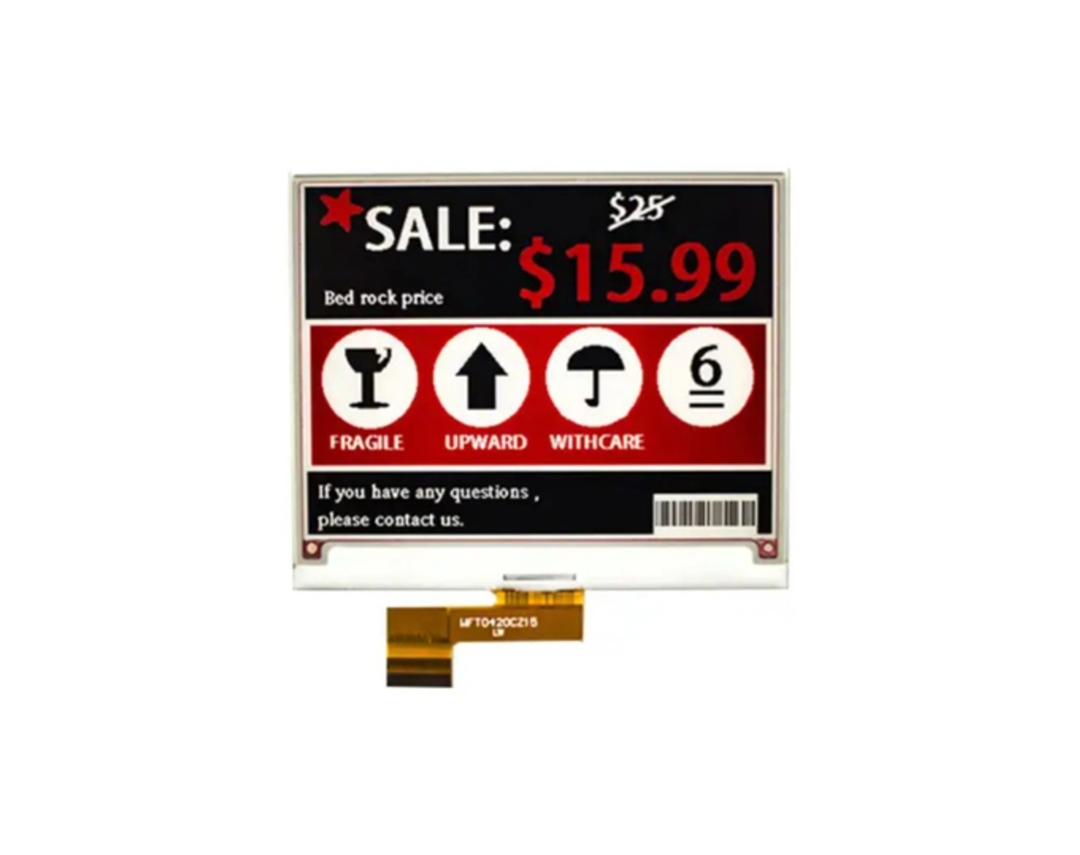
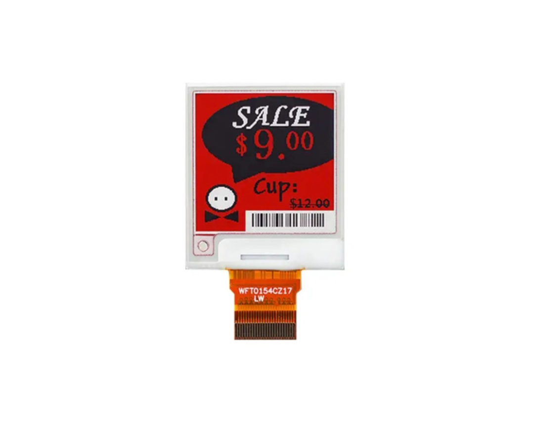
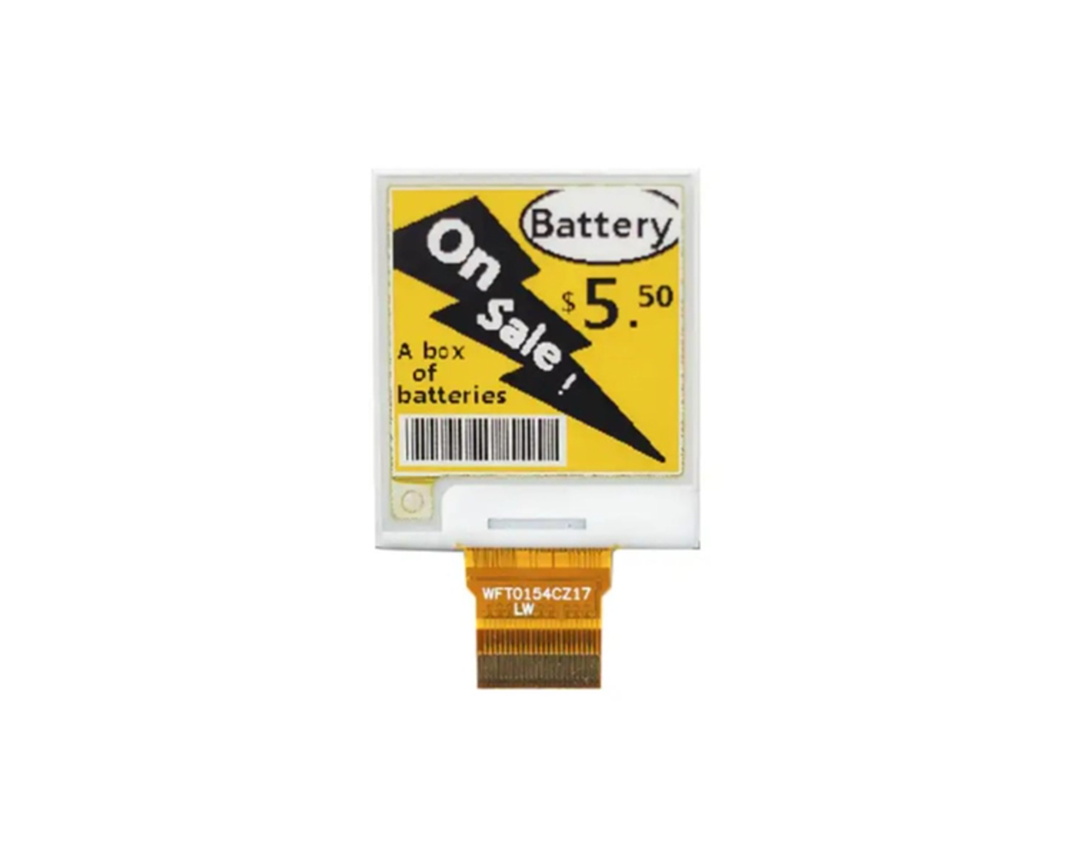
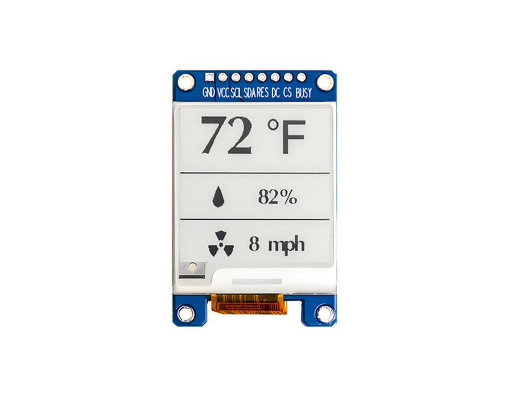
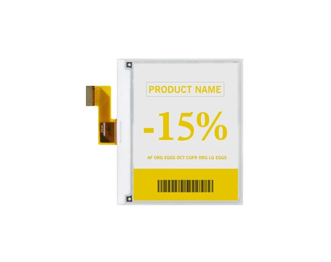
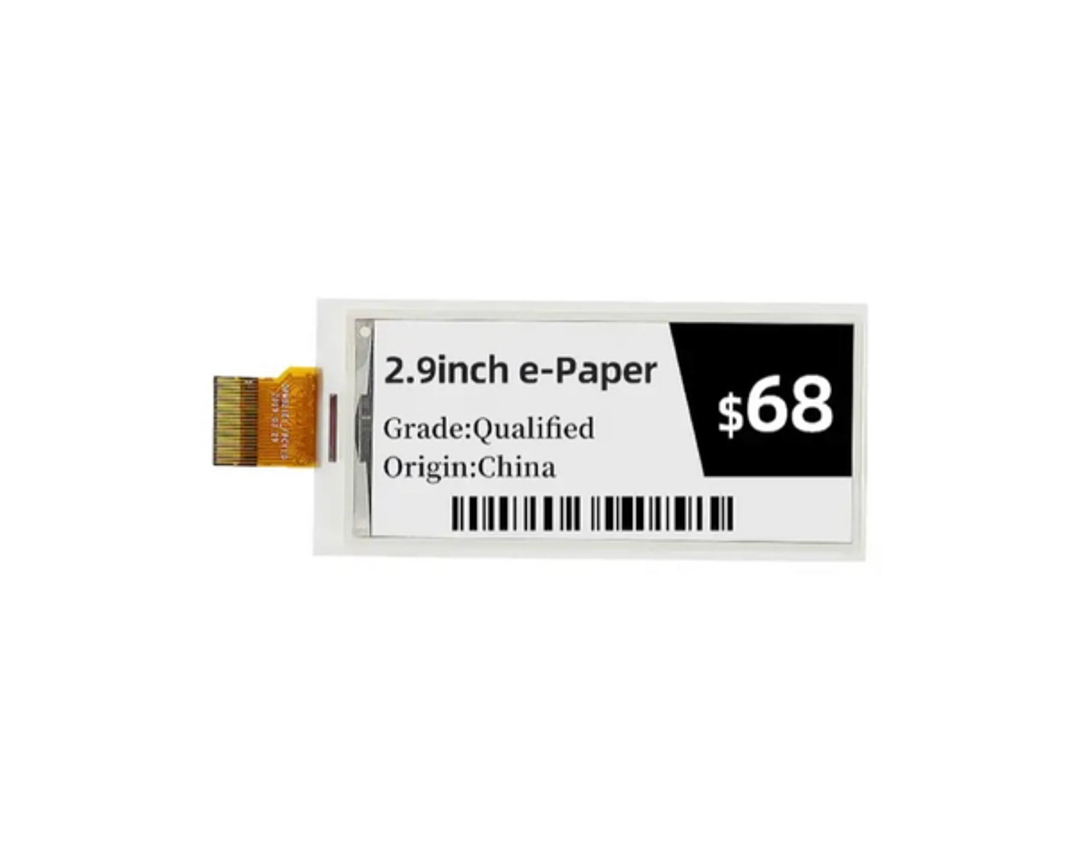
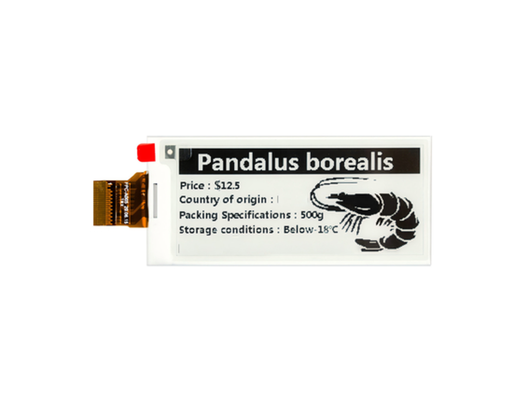
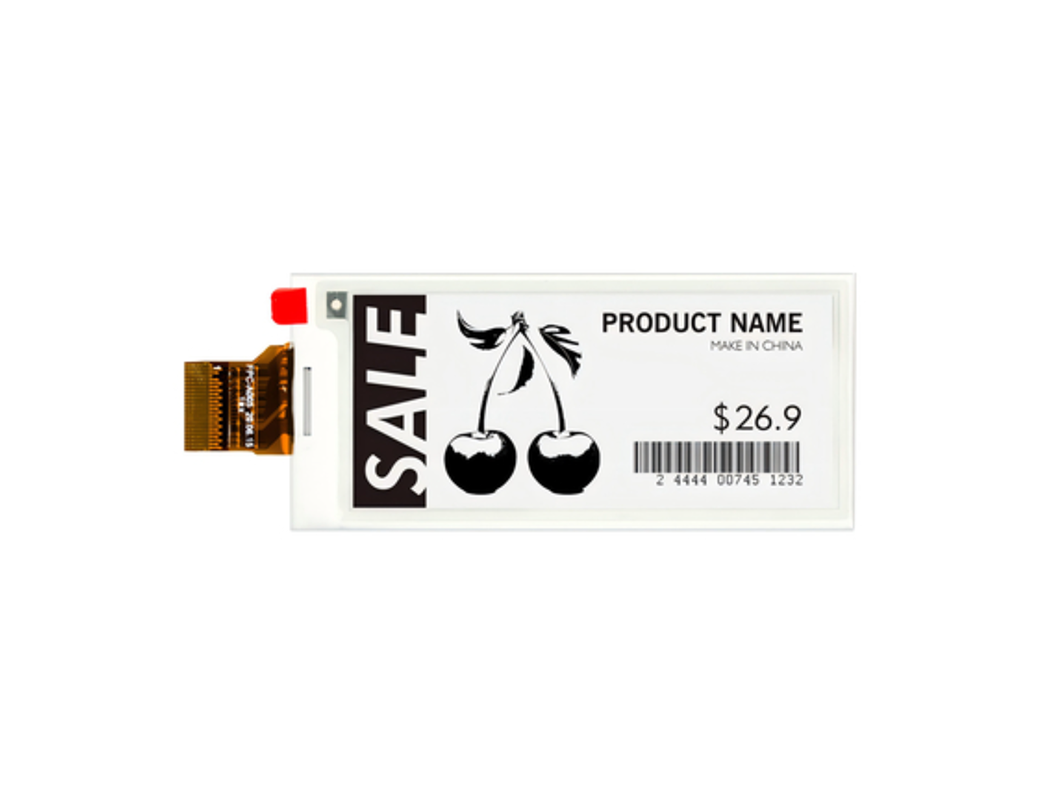
产品图像


手机/微信:135 0298 3321 柯先生
手机/微信:138 2960 7086 郑小姐
手机/微信:136 8686 7235 陈小姐
地址: 深圳市宝安区洲石路阳光工业区D栋


在线留言

 135 0298 3321
 首页 》
首页 》