高亮液晶屏
TFT触摸屏
HDMI TFT显示器
工业级TFT屏
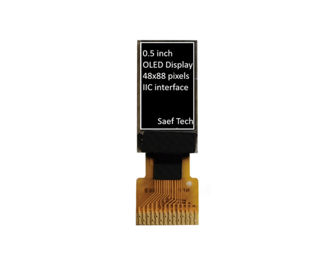
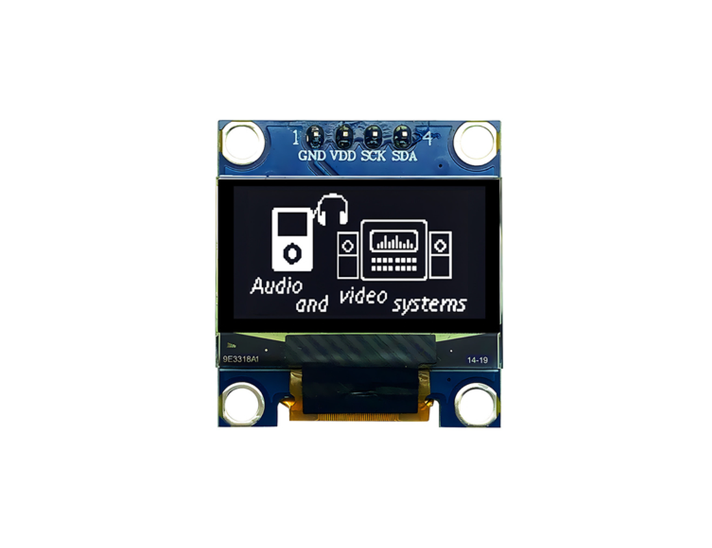
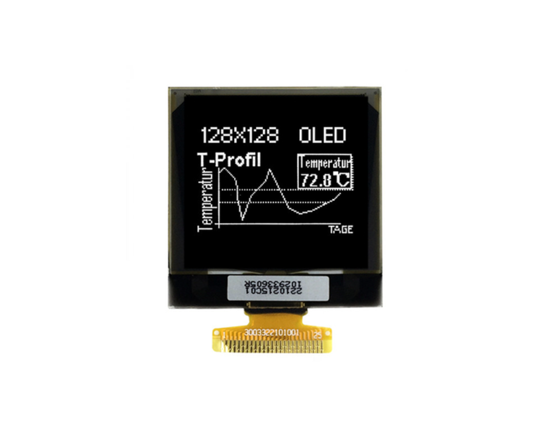
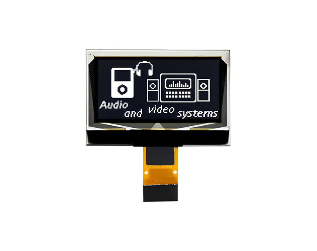
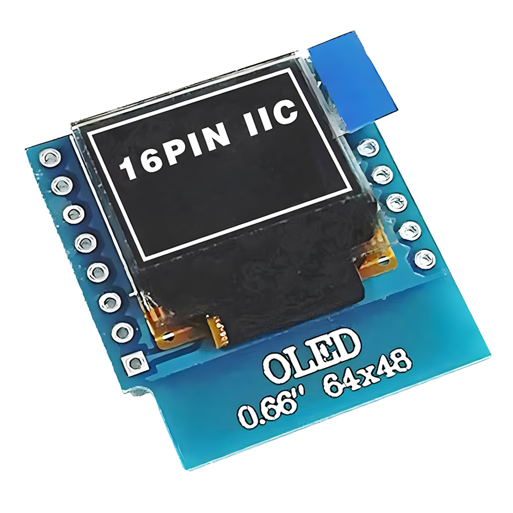
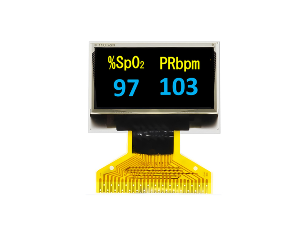
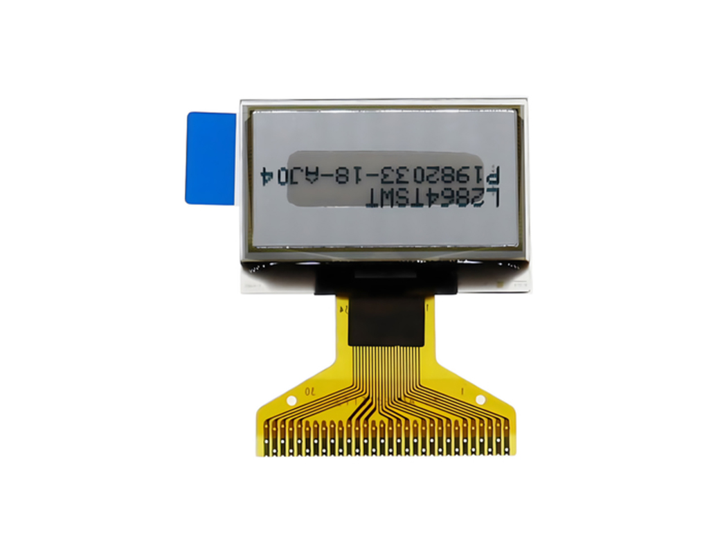
OLED屏
条型TFT屏
圆形TFT屏
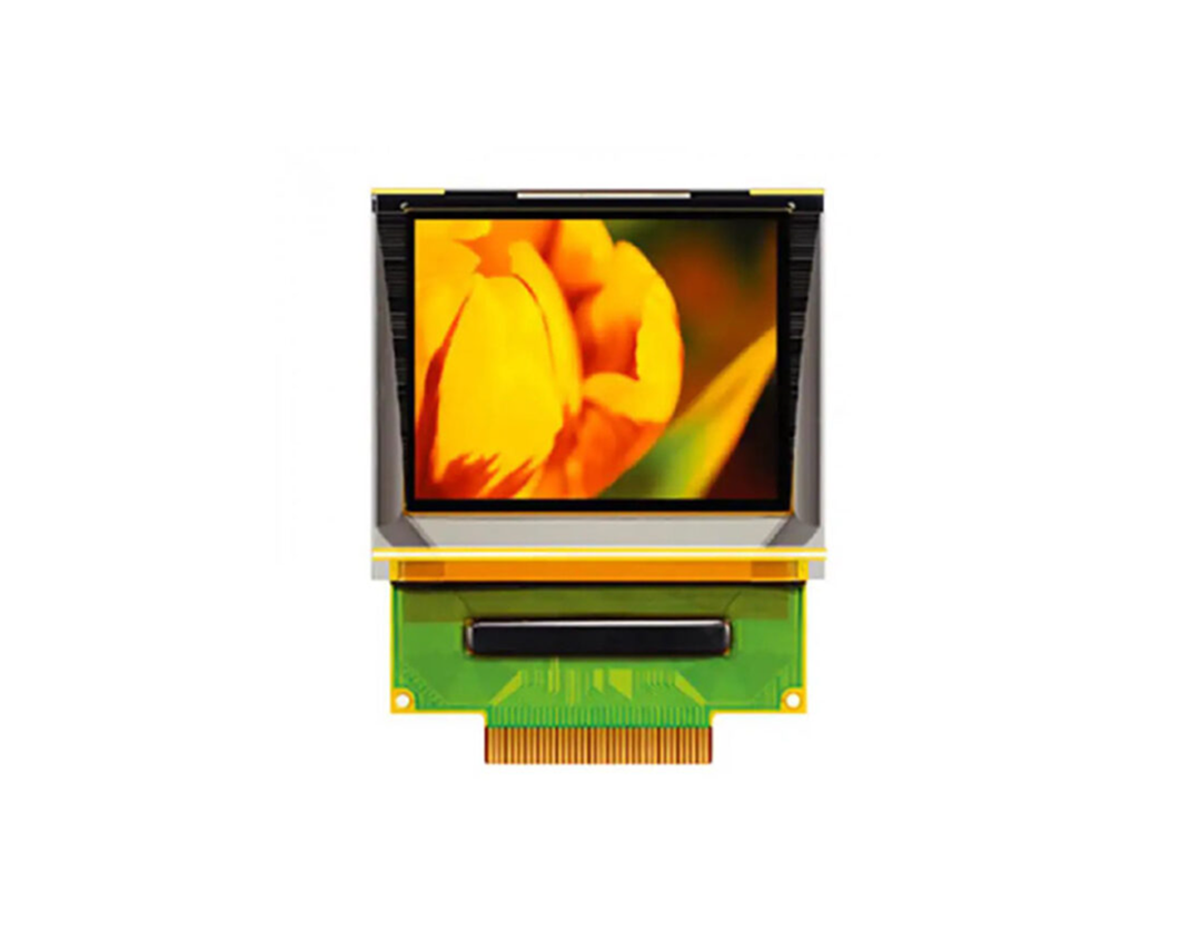
方形TFT屏
全视角TFT屏
电阻触摸TFT屏
电子墨水屏
树莓派触摸屏
OLED模块
高亮液晶屏
TFT触摸屏
HDMI TFT显示器
工业级TFT屏
OLED屏
条型TFT屏
圆形TFT屏
方形TFT屏
全视角TFT屏
电阻触摸TFT屏
电子墨水屏
树莓派触摸屏
OLED模块

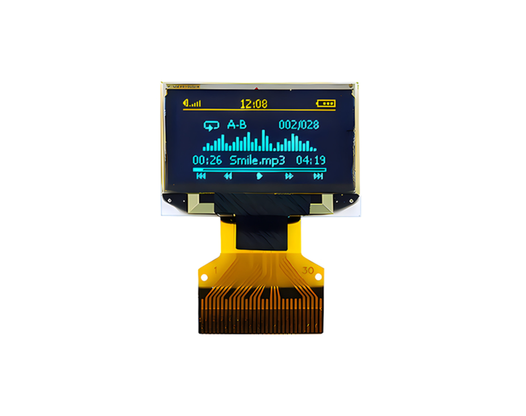
| Product: | 0.96" Inch Graphic OLED | Resolution: | 128x64 |
| Color: | Yellow+Blue (Dual Color) | Optics: | All Viewing Angles |
| Module Size: | 24.74*16.9*1.42 (mm) | Glass: | OLED |
| Controller: | SSD1315 | Operating Temp: | -40°C To +80°C |
| Pin Number: | 30 Pins | Interfaces: | 6800/8080 Parallel, 4-wire SPI, And I2C |
| Life Time: | 50,000 Hours | Brightness: | 180 Nits |
| Contrast Ratio: | 20,000 : 1 | Compliance: | REACH & RoHS Compliant |
| Highlight: | Dual Color Thin OLED Display, SPI Interface Thin OLED Display, SPI Interface Thin OLED Display | ||
0.96 英寸薄型 OLED 显示屏双色黄+蓝 SPI 接口产品介绍
产品快速回顾
►Model No. SFOS096JY-7149AN
►Thin OLED Display
►0.96" OLED Display, OLED 0.96"
►Suitable for wearable device
►Type: Graphic
►Structure: COG
►128 x 64 Dot Matrix
►IC:SSD1315
►3V Power supply
►1/64 duty
►Interface: 6800, 8080, SPI, I2C
►Display Color: Dual Color Yellow+Blue
描述
SAEF 发布了一款低成本 0.96 英寸薄型 OLED 显示屏 SFOS096JY-7149AN 型号,该型号由 128x64 像素组成,对角线尺寸仅为 0.96 英寸。新版薄型 0.96 英寸 OLED 显示屏还内置 SSD1315 驱动 IC;它通过 6800/8080 8 位并行和 I2C/SPI 接口进行通信。采用更薄的 OLED 面板是一种新趋势,对于新项目,我们建议客户为新设计项目选择更薄的 SFOS096JY-7149AN。SFOS096JY-7149AN 模块支持内部电荷泵供电和外部 VCC 供电。
产品信息
| Product: | 0.96" Inch Graphic OLED |
| Resolution: | 128x64 |
| Color: | Yellow+Blue (Dual Color) |
| Module Size: | 24.74*16.9*1.42 (mm) |
| Controller: | SSD1315 |
| Pin Number: | 30 Pins |
| Life Time: | 50,000 Hours |
| Contrast Ratio: | 20,000 : 1 |
| Optics: | All Viewing Angles |
| Glass: | OLED |
| Operating Temp: | -40°C To +80°C |
| Interfaces: | 6800/8080 Parallel, 4-wire SPI, And I2C |
| Brightness: | 180 Nits |
| Compliance: | REACH & RoHS Compliant |
0.96 英寸薄型 OLED 显示屏双色黄蓝 SPI 接口产品图

引脚定义
| No. | Symbol | Function |
| 1 | N.C. (GND) | Reserved Pin (Supporting Pin) The supporting pins can reduce the influences from stresses on the function pins. These pins must be connected to external ground. |
| 2 | C2P | Positive Terminal of the Flying Inverting Capacitor Negative Terminal of the Flying Boost Capacitor The charge-pump capacitors are required between the terminals. They must be floated when the converter is not used. |
| 3 | C2N | |
| 4 | C1P | |
| 5 | C1N | |
| 6 | VBAT | Power Supply for DC/DC Converter Circuit This is the power supply pin for the internal buffer of the DC/DC voltage converter. It must be connected to external source when the converter is used. It should be connected to VDD when the converter is not used. |
| 7 | NC | NC |
| 8 | VSS | Ground of Logic Circuit This is a ground pin. It acts as a reference for the logic pins. It must be connected to external ground. |
| 9 | VDD | Power Supply for Logic This is a voltage supply pin. It must be connected to external source. |
| 10 | BS0 | Communicating Protocol Select These pins are MCU interface selection input. See the following table:
|
| 11 | BS1 | |
| 12 | BS2 | |
| 13 | CS# | Chip Select This pin is the chip select input. The chip is enabled for MCU communication only when CS# is pulled low. |
| 14 | RES# | Power Reset for Controller and Driver This pin is reset signal input. When the pin is low, initialization of the chip is executed. |
| 15 | D/C# | Data/Command Control This pin is Data/Command control pin. When the pin is pulled high, the input at D7~D0 is treated as display data. When the pin is pulled low, the input at D7~D0 will be transferred to the command register. For detail relationship to MCU interface signals, please refer to the Timing Characteristics Diagrams. When the pin is pulled high and serial interface mode is selected, the data at SDIN is treated as data. When it is pulled low, the data at SDIN will be transferred to the command register. In I2C mode, this pin acts as SA0 for slave address selection. |
| 16 | R/W# | Read/Write Select or Write This pin is MCU interface input. When interfacing to a 68XX-series microprocessor, this pin will be used as Read/Write (R/W#) selection input. Pull this pin to “High” for read mode and pull it to “Low” for write mode. When 80XX interface mode is selected, this pin will be the Write (WR#) input. Data write operation is initiated when this pin is pulled low and the CS# is pulled low. |
| 17 | E/RD# | Read/Write Enable or Read This pin is MCU interface input. When interfacing to a 68XX-series microprocessor, this pin will be used as the Enable (E) signal. Read/write operation is initiated when this pin is pulled high and the CS# is pulled low. When connecting to an 80XX-microprocessor, this pin receives the Read (RD#) signal. Data read operation is initiated when this pin is pulled low and CS# is pulled low. |
| 18~25 | D0~D7 | Host Data Input/Output Bus These pins are 8-bit bi-directional data bus to be connected to the microprocessor’s data bus. When serial mode is selected, D1 will be the serial data input SDIN and D0 will be the serial clock input SCLK. When I2C mode is selected, D2 & D1 should be tired together and serve as SDAout & SDAin in application and D0 is the serial clock input SCL. |
| 26 | IREF | Current Reference for Brightness Adjustment This pin is segment current reference pin. A resistor should be connected between this pin and VSS. Set the current lower than 12.5μA. |
| 27 | VCOMH | Voltage Output High Level for COM Signal This pin is the input pin for the voltage output high level for COM signals. A capacitor should be connected between this pin and VSS. |
| 28 | VCC | Power Supply for OEL Panel This is the most positive voltage supply pin of the chip. A stabilization capacitor should be connected between this pin and VSS when the converter is used. It must be connected to external source when the converter is not used. |
| 29 | VLSS | Ground of Analog Circuit This is an analog ground pin. It should be connected to VSS externally. |
| 30 | NC (GND) | Reserved Pin (Supporting Pin) The supporting pins can reduce the influences from stresses on the function pins. These pins must be connected to external ground. |
0.96 英寸薄型 OLED 显示屏双色黄蓝 SPI 接口产品图


工厂设施和证书


手机/微信:135 0298 3321 柯先生
手机/微信:138 2960 7086 郑小姐
手机/微信:136 8686 7235 陈小姐
地址: 深圳市宝安区洲石路阳光工业区D栋


在线留言

 135 0298 3321
 首页 》
首页 》